Photos
Published:
I’ll post some interesting pictures I’ve taken here. Oh the beauties of nanofabrication….
2025 January: I’m switching from a bare Silicon substrates to Silicon substrates with markers. Twofold reasons:
- I’ll track the same 2D material flake across a range of processes. Easier to find under microscopes and perform PL scans
- Easier communication about the samples. Also if I ship my samples to someone they can use the same benefits.
2024 November: I’m switching from a simple design of 1 waveguide per 2-in sapphire wafer to 28 per wafer. Threefold reasons:
- My newer samples don’t need as high MW power as before so I can make do with wirebonding.
- I can make ~28 usables samples from 1 chip, which means I don’t have to do fabrication as often.
- I save $$$s.
2024 September: This is an SEM image of a nanotube we loaded onto an AFM tip from my Nature Communications paper. What a beauty indeed! The scale bar is 2 $\mu$ m. This was a pain to figure out and perform. 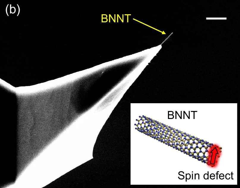
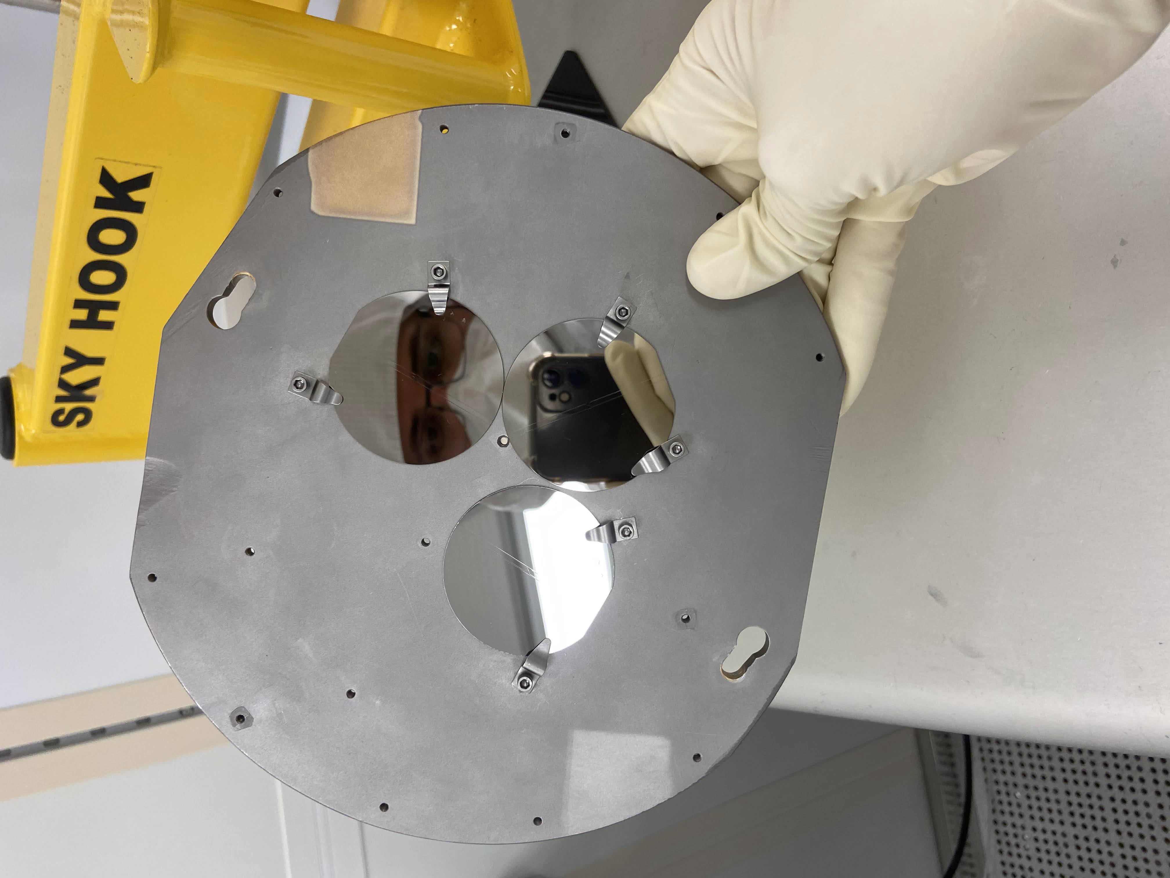
2023 October: Successful fabrication of some test wafers for my optical measurements. Yes, that is me in the reflection and I am wearing a clean room suit.