
Research
Over the years I have worked on a bunch of projects. Here’s a list and a bit of information about them.
You can find my articles on Google Scholar.
2026: Quantum Sensing of Opaque Materials with Plasmonically Enhanced Hexagonal Boron Nitride Spin Defects
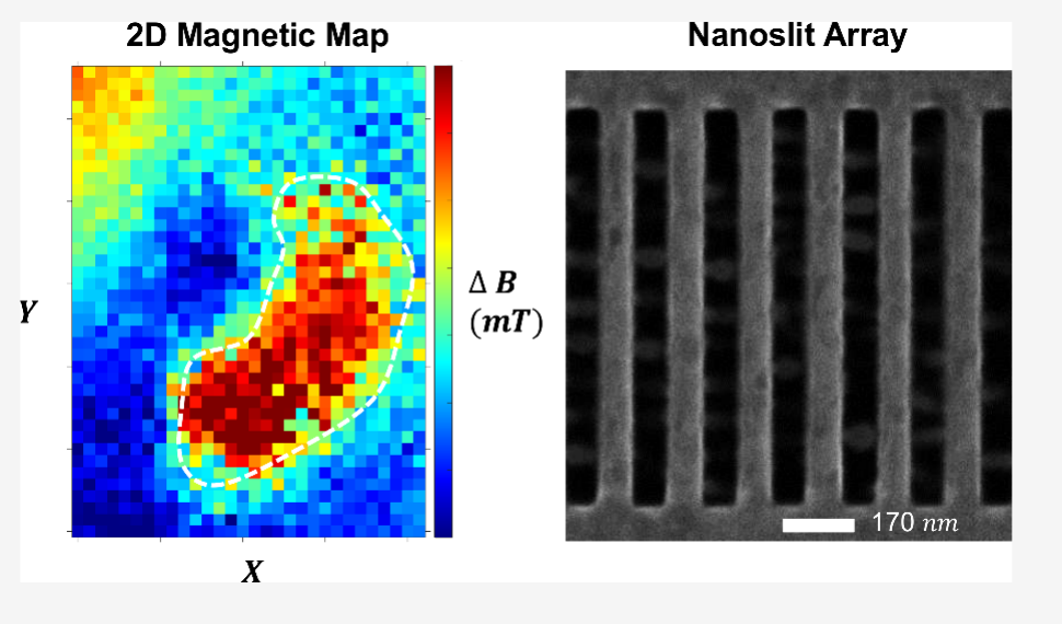
Sensing through opaque or scattering materials (like battery casings) is a major limitation for conventional quantum sensors, since the material blocks optical access to the spin defect. We design and nanofabricate a coplanar waveguide integrated with nanoslit arrays patterned through a thin gold film using a focused ion beam, enabling back-side excitation and photoluminescence collection from hBN spin defects while simultaneously delivering microwaves and providing plasmonic enhancement. We demonstrate the device by performing $T_1$ relaxometry and magnetic field mapping of nickel nanoparticles, extending plasmonically-enhanced quantum sensing to opaque systems and liquids such as lithium-ion batteries.
Check out the published paper in Nano Letters, or read the PDF directly.
2026: Coupling Nanostructured Plasmon-Strain Microwave Waveguide to Spin Defects in Hexagonal Boron Nitride for High-Sensitivity Quantum Sensors
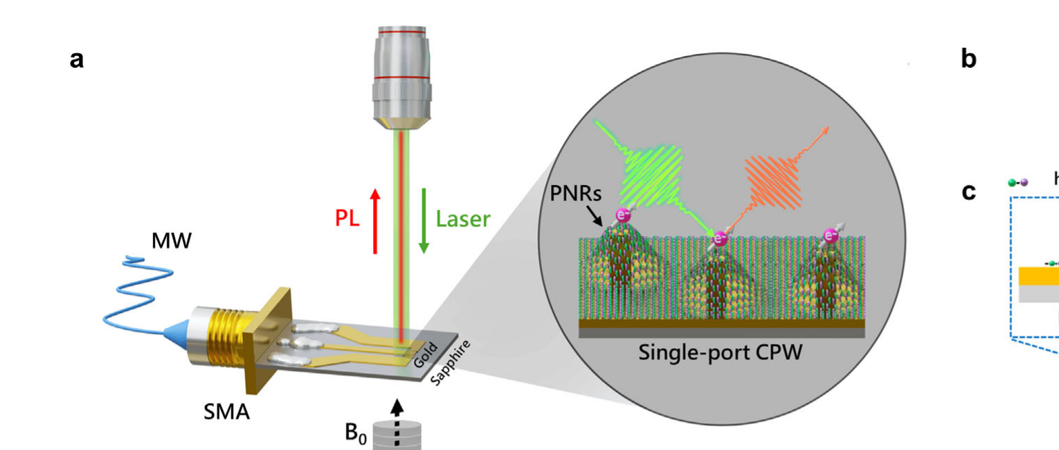
The intrinsically low optical quantum yield of the $V_B^-$ spin defect in hBN limits sensor sensitivity despite hBN’s easy on-chip integration. We fabricate arrays of alumina-coated gold nanopillars onto the constricted region of a microwave-efficient, single-port gold coplanar waveguide. The alumina coating suppresses photoluminescence quenching while the gold nanopillars enhance local electromagnetic fields and induce strain-driven perturbations of the defect energy levels, boosting photo-emission. This yields a roughly tenfold enhancement in photoluminescence and improves optically detected magnetic resonance contrast to ~17%, achieving a DC magnetic field sensitivity of 9.4 uT/root-Hz, among the best reported for $V_B^-$ defects.
Check out the published paper in Advanced Materials, or read the PDF directly.
2025: Room-temperature quantum entanglement in a van der Waals material

Entangling qubits in van der Waals materials had remained elusive, despite these materials’ promise for nanoscale quantum sensing. We report room-temperature quantum entanglement between an optically addressable electron spin and a strongly coupled $^{13}$C nuclear spin in hexagonal boron nitride. By extending the electron spin coherence to 38 microseconds with dynamical decoupling, we create maximally entangled Bell states with a fidelity up to 0.89, and use the nuclear spin as a long-lived quantum memory to enhance AC magnetic field sensing via correlation spectroscopy. This establishes entangled spin qubits in hBN as a robust platform for advanced quantum technologies based on 2D materials.
Check out the paper on Arxiv, or read the PDF directly.
2025: Quantum sensing with a spin ensemble in a van der Waals material
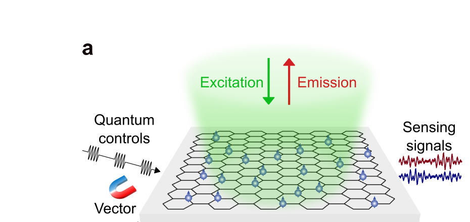
In collaboration with Stanford University, we present a comprehensive experimental framework for probing a 2D spin ensemble’s Hamiltonian, coherent sensing dynamics, and noise environment. Using a central spin system in an hBN crystal, we fully map the hyperfine interactions with proximal nuclear spins, demonstrate switchable magnetic and electric noise sensing, and introduce a method to accurately reconstruct the environmental noise spectrum. We achieve a record coherence time of 80 microseconds under dynamical decoupling, enabling sub-microtesla AC magnetic sensitivity at a 10 nm target distance, rivaling state-of-the-art diamond NV platforms without the need for complex surface treatment.
Check out the paper on Arxiv, or read the PDF directly.
2025: Single nuclear spin detection and control in a van der Waals material
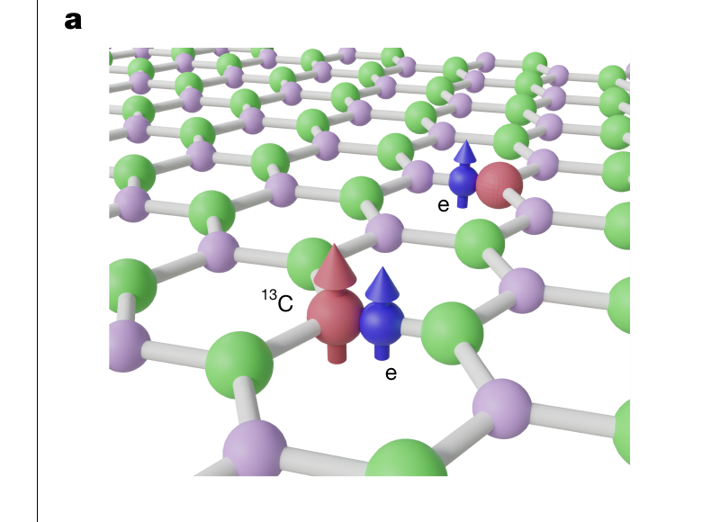
We’ve found single electron-nuclear spin coupling in hexagonal Boron Nitride. This is the first such demonstration in a 2D material. We create single spin defects in hBN using $^{13}$C ion implantation, identify three distinct defect types based on hyperfine interactions, and observe both $S=1/2$ and $S=1$ spin states within a single hBN spin defect. We demonstrate atomic-scale NMR and coherent control of individual nuclear spins with a pi-gate fidelity up to 99.75% at room temperature, and by comparing experiments with DFT calculations, propose chemical structures for these defects. Possible applications of this research would be in quantum communication and on-chip quantum sensing.
Check out the published paper in Nature, or read the PDF directly.
2025: Spin-State-Selective Excitation in Spin Defects of Hexagonal Boron Nitride
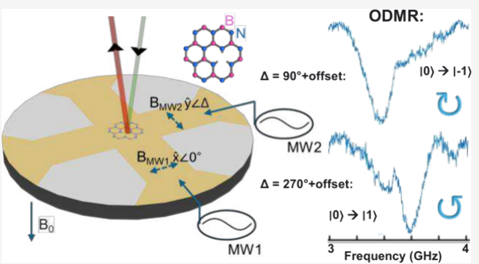
Spectral overlap of spin transitions due to large hyperfine interactions has limited the magnetic sensitivity of the $V_B^-$ defect in hBN. We demonstrate spin-selective excitation of $V_B^-$ spin defects driven by circularly polarized microwaves. Using a cross-shaped microwave resonance waveguide, we superimpose two orthogonally linearly polarized microwaves shifted in phase from an FPGA to generate circularly polarized microwaves, enabling selective excitation of individual spin transitions as confirmed by optically detected magnetic resonance and supported by computation. This enhances the hBN platform for quantum sensing through better spin state control and magnetic sensitivity at low and zero fields.
Check out the published paper in Nano Letters, or read the PDF directly.
2025: A Power-Efficient Coplanar Waveguide Design for Enhanced Optical Readout in h-BN Quantum Sensors
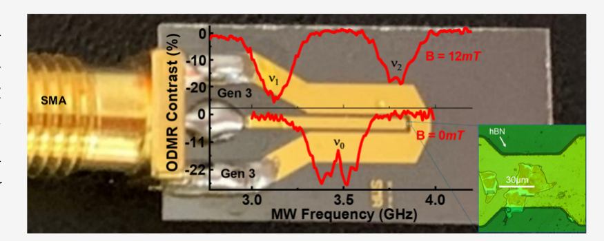
Current hBN quantum sensing devices suffer from low optical readout and noisy signals due to inefficient waveguide designs that limit microwave absorption and reduce optically detected magnetic resonance (ODMR) contrast. We advance hBN-integrated quantum sensors through three generations of design, culminating in a compact single-port coplanar waveguide that allows on-chip optical and microwave excitation, improving impedance stability and RF magnetic field concentration without altering spin properties. This achieves an ODMR contrast of ~28% at low microwave power (400 mW), a threefold efficiency enhancement that reduces RF power use by up to five times, making it ideal for scalable quantum sensing applications such as magnetic field detection.
Check out the published paper in Nano Letters, or read the PDF directly.
2025: Coherent Spins in van der Waals Semiconductor GeS2 at Ambient Conditions
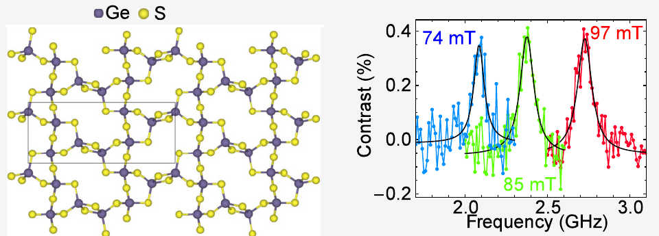
We report the observation and room-temperature coherent control of ensemble spin defects in the high-temperature crystalline phase of germanium disulfide (beta-GeS2), a 2D semiconductor with low nuclear spin density. The defects exhibit spin-1/2 behavior, and their dynamics can be explained by a weakly coupled spin-pair model. We implement dynamical decoupling techniques to extend the coherence time ($T_2$) by a factor of 20, and use DFT calculations to estimate the structures and spin densities of two possible spin defect candidates. This work helps expand the field of quantum sensing with spin defects in 2D materials beyond hBN.
Check out the published paper in Nano Letters, or read the PDF directly.
2025: Roadmap: 2D Materials for Quantum Technologies

Two-dimensional materials have emerged as a versatile and powerful platform for quantum technologies, offering atomic-scale control, strong quantum confinement, and seamless integration into heterogeneous device architectures. This Roadmap, written with collaborators across many institutions, provides a comprehensive overview of recent progress and future directions in exploiting 2D materials for quantum sensing, computation, communication, and simulation, surveying spin defects, quantum emitters, nonlinear photonics, spintronic and magnonic devices, superconducting and hybrid quantum circuits, quantum dots, Moire quantum simulators, and quantum communication platforms.
Read the PDF directly (Arxiv link TBD).
2024: Nanotube Spin Defects for Omnidirectional Quantum Sensing
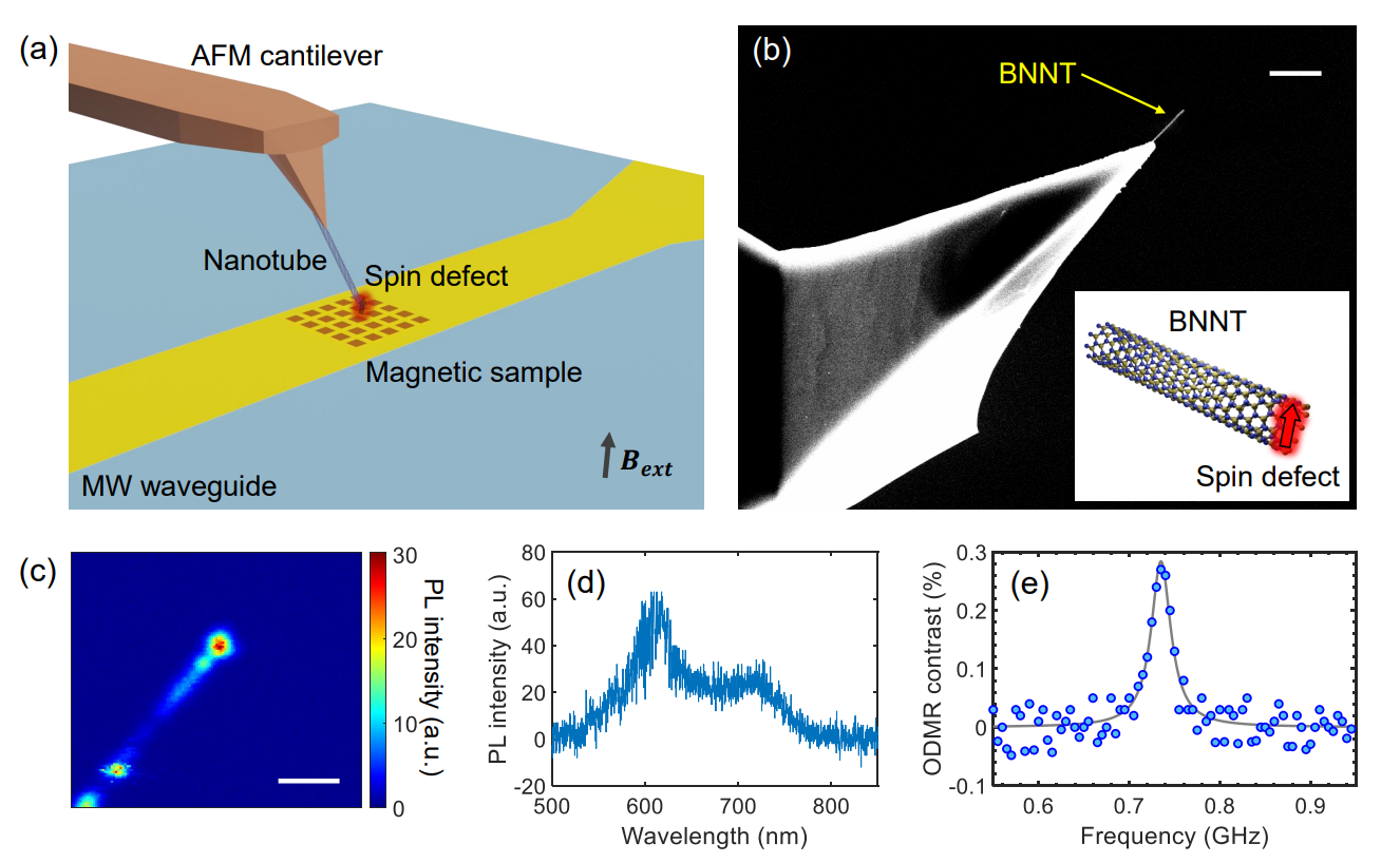
Conventional quantum magnetometers (e.g. diamond NV, hBN $V_B^-$) have a preferential axis of maximum sensitivity, which limits their utility for sensing magnetic fields. We have discovered spin defects in Boron Nitride Nanotubes with omnidirectional sensitivity. We build on this by further developing a near-surface magnetic scanning microscope. We also invent a technique to reliably transfer a BNNT to an AFM tip, which turns the tip into a scanning quantum sensor. This can potentially be used to perform two-in-one magnetic map and surface profile measurements at the atomic scale.
To learn more check out the published paper in Nature Communications, or read the PDF directly.
2023: Quantum sensing of paramagnetic spins in liquids with spin qubits in hexagonal boron nitride
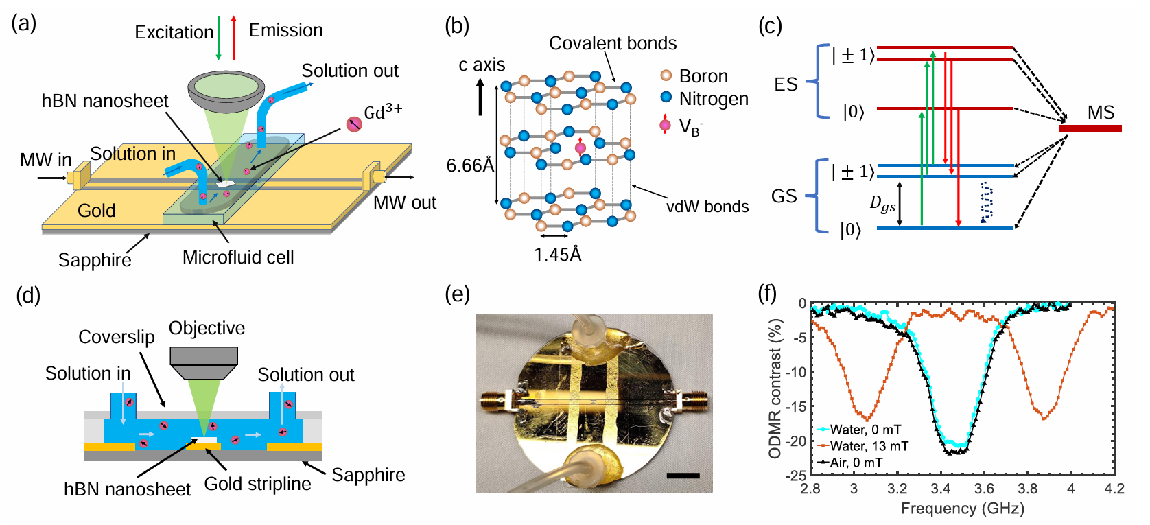
We show a practical application of quantum sensing for real-world applications by using spin defects in Boron Nitride to detect small concentrations of paramagnetic ions in a liquid solution. We combine a microfluid cell with optical readout of the quantum sensors to interface the paramagnetic ions with the sensor. We show we can detect as few as $10^5$ ions in a small volume inside the focus of the laser. This has potential applications for building noninvasive all-optical sensors for ions in liquid solutions.
Check out the published paper in ACS Photonics, or read the PDF directly.
2023: Quantum sensing and imaging with spin defects in hexagonal boron nitride

Color centers in hexagonal boron nitride (hBN) have emerged as promising candidates for a new wave of quantum applications. Thanks to hBN’s high stability and 2D layered structure, color centers in hBN can be readily integrated into nanophotonic and plasmonic structures on a chip. This review summarizes the rapidly evolving field of quantum sensing with spin defects in hBN, introducing basic properties of hBN spin defects, quantum sensing protocols, and recent experimental demonstrations of quantum sensing and imaging, methods to enhance their sensitivity, and potential future developments and applications.
Check out the published review in Advances in Physics: X, or read the PDF directly.
2022: Nuclear spin polarization and control in hexagonal boron nitride
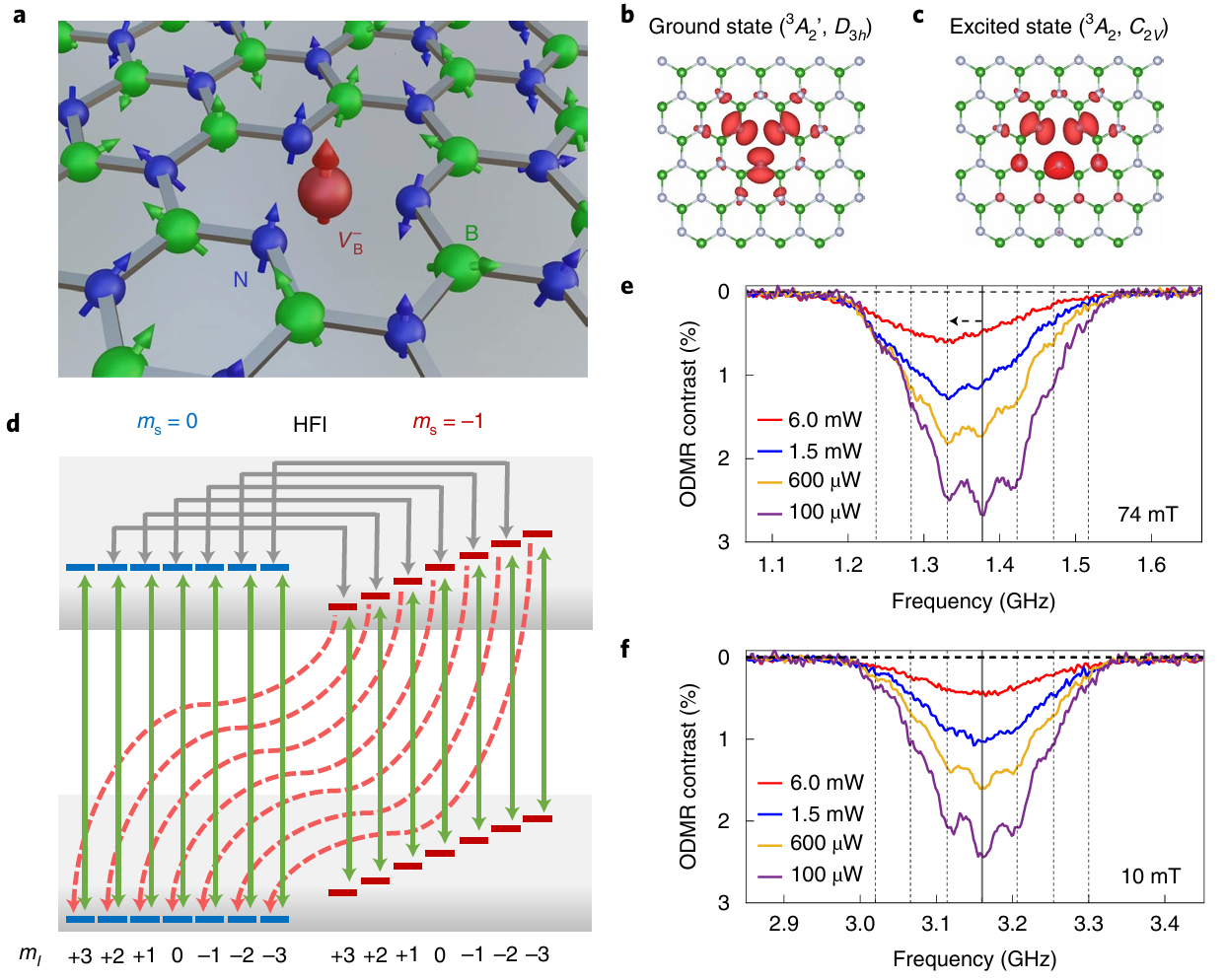
The $V_B^-$ spin defect in hexagonal Boron Nitride is emerging as a prominent solid-state spin qubit system for quantum sensing applications. We demonstrate the polarization and control of the nitrogen nuclei surrounding the $V_B^-$ spin defect, and show that we can achieve 32% polarization under laser excitation in a magnetic field. This opens up new avenues for quantum sensing, communication and networks.
Check out the published paper in Nature Materials, or read the PDF directly.
2022: Light induced quasi-Fermi level splitting in molecular semiconductor alloys
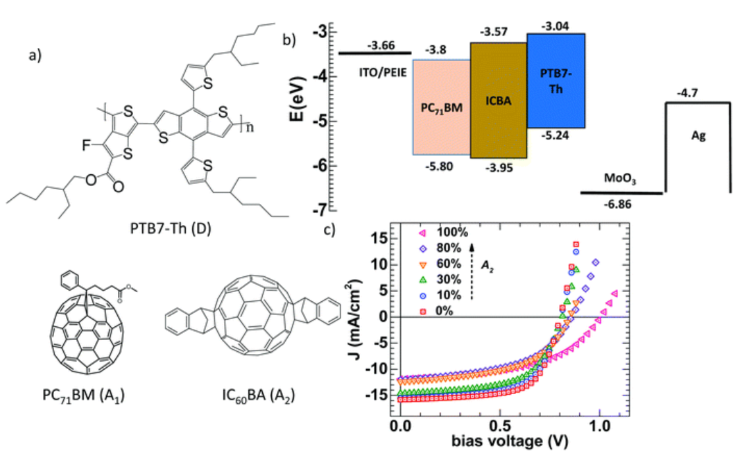
We study the quasi-Fermi level splitting in a series of ternary blended solar cells. We also propose an analytical model based on the photoinduced fermion occupancy based on experimental observations. This is then generalizable to a range of excitonic molecular semiconductor-based solar cells.
2022: Autoencoders for Denoising of Poisson Noise Limited Biological Images
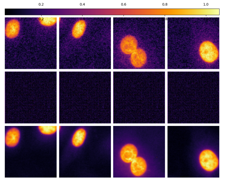
Variational Autoencoders (VAE) have been used to denoise images with Gaussian Noise. The noise in the images is assumed to be drawn from a Gaussian distribution. Autoencoders can reduce the dimensionality of large-sized complex data and then reconstruct it back with minimal loss. By tuning the training process and adding a Gaussian noise component the encoder-decoder system can be made into an effective denoiser. Here we present an extension of this concept for non-Gaussian noise, in this case, Poisson noise, typically generated in images where the amount of incident light per pixel is very small. Such low photon number images are generated in the imaging of biological samples under low light excitation. The physical model is captured in the weights of the autoencoder and deploying it for noise reduction yields a good method to reduce complex computation.
2021: Novel optoelectronic technique for direct tracking of ultrafast triplet excitons in polymeric semiconductor
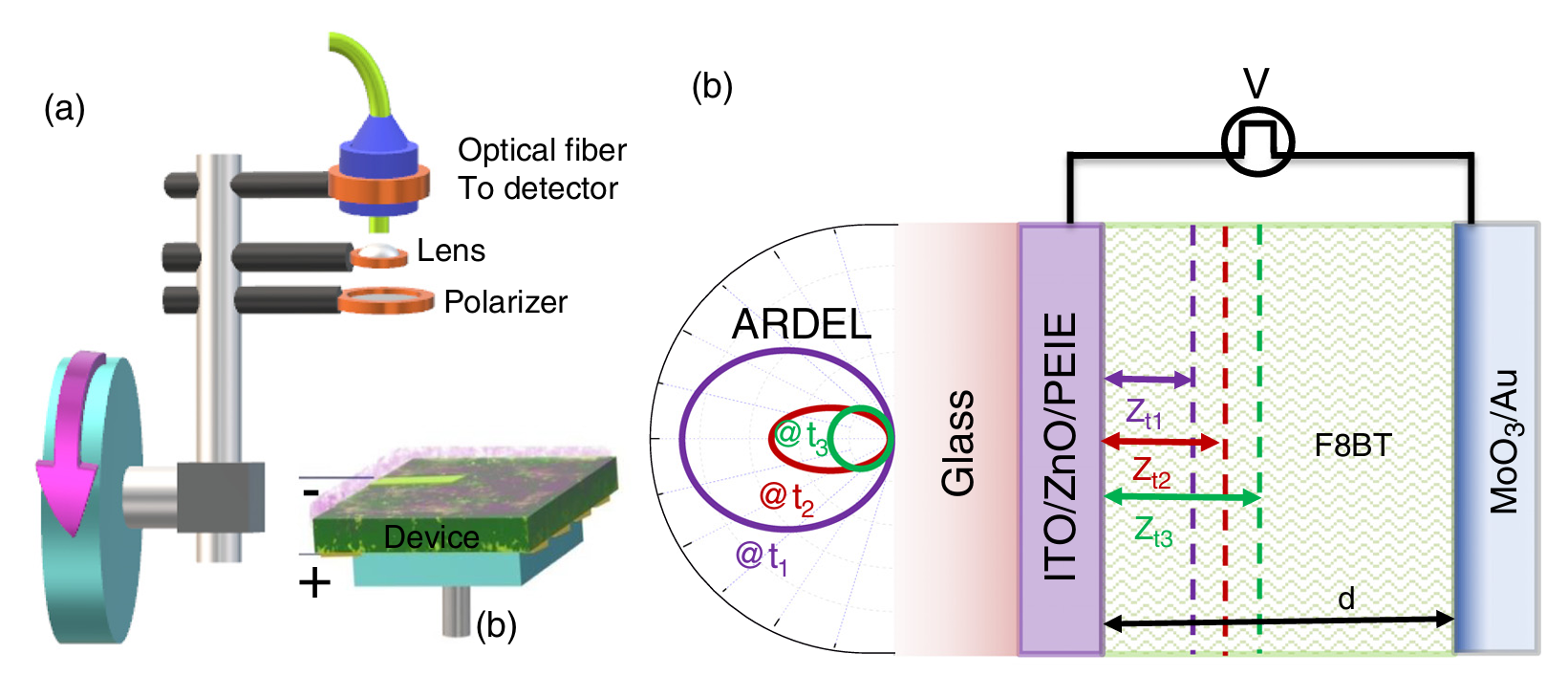
We study the effect of polymer chain packing on triplet diffusion in the polyfluorene-based polymeric system, which is known to give efficient organic light emitting diode (OLED) efficiency for display devices. We have developed a unique method to trace the position of the triplet exciton in the emissive layer of OLEDs by analyzing angle-resolved delayed electroluminescence emission patterns as a function of time, by fitting the observed profiles with the calculated profiles given a certain depth distribution. This study paves a path for better engineering of OLED devices by enabling a better understanding of charge carrier dynamics.